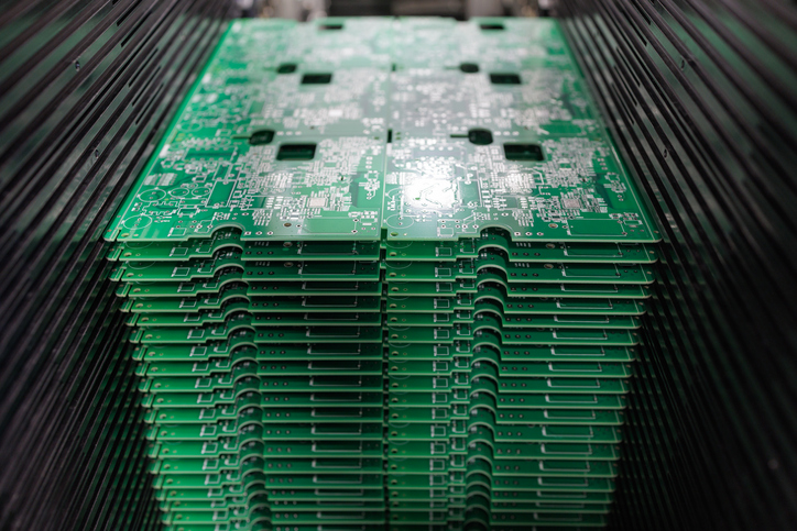
Automated optical inspection (AOI) is a quality control process that uses a machine to perform visual inspection during or after the manufacturing process. This advanced technology helps identify issues early, improving reliability and reducing production costs. By implementing PCB AOI inspection, companies can maintain high production standards and minimize the risk of faulty products reaching customers.
Industrial control and automation electronics operate under harsh conditions but require a high level of reliability. The printed circuit boards inside PLCs, motor drives, HMI panels, sensor interfaces, and power distribution modules must function for years in environments experiencing temperature swings, vibration, dust, electrical noise, and continuous duty cycles. PCB AOI inspection helps ensure reliable field performance and prevent latent defects.
The Benefits of PCB AOI Inspection
Automated optical inspection (AOI) significantly improves the quality and efficiency of electronics manufacturing by automating defect detection that might otherwise go unnoticed during manual checks. Instead of relying on human inspectors, AOI can rapidly scan printed circuit boards (PCBs) for issues such as missing components, incorrect placement, misalignments, and soldering errors.
The technology delivers higher precision and repeatability, ensuring that even subtle defects are identified early in the production process. This early detection helps prevent costly rework and reduces the likelihood of faulty products reaching customers. AOI provides consistent, non-contact inspection, which is especially valuable for high-density boards with complex layouts, maximizing yields and supporting high production standards.
Key benefits of PCB AOI inspection include:
- Improved quality and accuracy – AOI can detect very small defects that are often missed by the human eye.
- Efficiency – Complex boards can be inspected significantly faster than manual inspection
- Cost-Effective – Identifying defects early reduces expensive rework, scrap, and material waste.
- Data Collection – The system generates large amounts of data that can be used to improve processes and quality.
How AOI Works in Electronics Manufacturing
AOI is used in electronics manufacturing to verify that components and solder joints match the design intent after placement and reflow. AOI relies on controlled imaging, lighting, and measurement algorithms to detect defects consistently across every board. The system measures geometry, contrast, height, and position against known references.
AOI compares the physical PCB to expected conditions derived from CAD data, centroid files, and learned reference images. The inspection is quantitative, not subjective.
AOI typically measures:
- Component presence and position – The system verifies that each component exists, is placed within tolerance, and is aligned correctly relative to pads and silkscreen. X-Y offset, rotation, skew, and polarity are evaluated against defined limits.
- Component geometry – Length, width, and footprint outline are measured to confirm that the correct package type was installed. This is how wrong-part or swapped-part errors are detected.
- Solder joint characteristics – AOI evaluates solder volume, shape, and coverage. Depending on the inspection method, this includes fillet height, wetting angle, solder spread, and symmetry between pads.
- Height and coplanarity – In 3D systems, height data is captured to detect lifted leads, floating components, insufficient solder, or warped packages. Coplanarity checks are critical for fine-pitch devices and gull-wing leads, where electrical contact may appear acceptable from above but fail mechanically.
- Surface anomalies – The system looks for solder balls, bridges, opens, tombstones, flipped components, and foreign material based on contrast and shape deviations.
The system uses side cameras to address limitations of top-down imaging. Many critical solder joints are partially or fully obscured when viewed only from above. By capturing oblique or near-horizontal views, side cameras provide visibility into solder joint formation that cannot be inferred reliably from height data alone. This reduces false passes on marginal joints and lowers false calls caused by top-down ambiguity. Side cameras are not used for every component. They are typically applied selectively based on package type and risk profile.
AOI does not make a pass/fail decision based on a single image. It evaluates multiple measurements per component and applies rules based on manufacturing tolerances.
Contact SMTNW For Industrial Control and Automation Electronics
At SMTNW, we build industrial control and automation electronics with the expectation that boards will operate continuously in harsh, uptime-critical environments, so inspection is treated as a core process control, not a downstream check. We run 100 percent PCB AOI inspection on every assembly, using 3D AOI to measure component presence, placement accuracy, solder volume, coplanarity, and other physical attributes that directly affect long-term reliability in control systems.
That data is used to identify variation early, tighten process windows, and prevent defects from escaping into the field, which is essential for automation electronics where failures are costly, difficult to diagnose, and rarely tolerated. To learn how our manufacturing and quality control processes can reduce your risk, contact us.